GeForce 4 Ti 4200
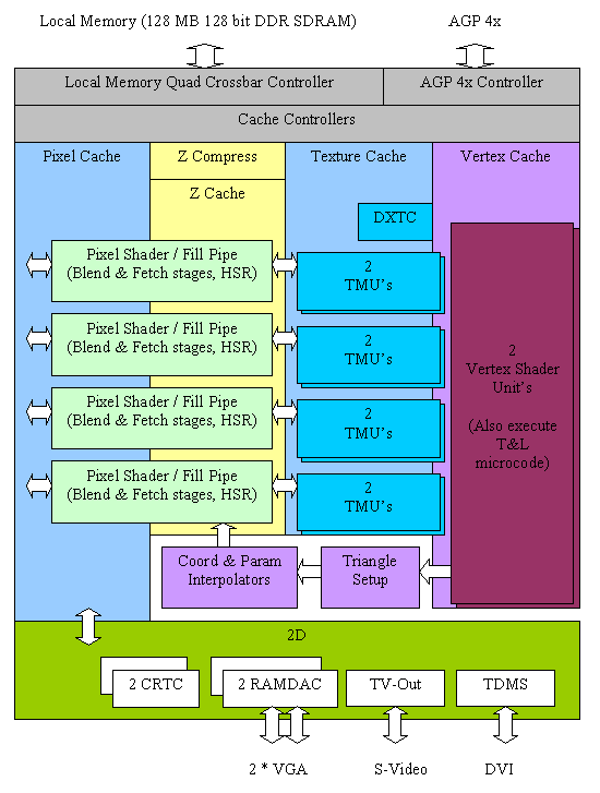
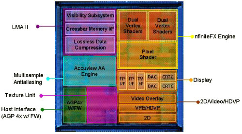
Main architectural innovations of NV25 (compared to NV20)
Two independent display controllers (CRTCs). Flexible support for various modes with the output of two frame buffers independent in resolution and content to any available signal receivers.
Two full-fledged 350 MHz RAMDACs integrated into the chip (with a 10-bit palette).
Chip-integrated TV-out interface.
TDMS transmitter integrated into the chip (for DVI interface).
Two blocks for interpreting and executing vertex shaders. They promise a significant increase in the speed of processing scenes with complex geometry. Blocks cannot use different microcode shaders, the only purpose of such duplication - processing two vertices at the same time - is to increase performance.
Improved rendering pipelines provide hardware support for pixel shaders up to and including version 1.3.
According to NVIDIA, the effective fill rate in MSAA modes has been increased, now 2x AA and Quincunx AA modes will cause a significantly smaller performance drop. Slightly improved Quincunx AA (shifted sampling positions). A new AA method has appeared - 4xS.
Improved separate cache system (4 separate caches for geometry, textures, frame buffer and Z buffer).
Advanced lossless compression (1:4) and fast clearing of the Z buffer.
Improved Hidden Surface Rejection Algorithm (Z Cull HSR).
Summing up this list, I would like to note the evolutionary rather than revolutionary nature of the changes in comparison with the previous creation of NVIDIA (NV20). However, this is not surprising - historically, NVIDIA first offered a product that carried many new technologies, and then released a more advanced (optimized) version based on it, eliminating the shortcomings that attracted the main attention (during the presence of the product on the market).
Structural diagram of N25
According to the testing carried out after the release of video cards, the GeForce4 Ti turned out to be noticeably faster than the GeForce3 Ti. Such an impressive gap in NV25 performance was achieved not due to some fundamentally new technology, but due to further debugging and tweaking of technologies existing in GeForce3 (NV20). Bear in mind that the GeForce4 core was only 5% larger than the NV20 core with the same manufacturing process (0.15 µm).
nfiniteFX II vertex shaders
If the GeForce3 had only one vertex shader module, then the GeForce4 Ti has two of them. However, this is unlikely to surprise you, since the nVidia chip for the Microsoft Xbox also has two vertex shader modules. Unless the modules have been improved in NV25.
Obviously, two parallel vertex shader modules could process more vertices per unit of time. To do this, the chip itself decomposed the vertices into two streams, so the new mechanism is transparent to applications and APIs. Instruction scheduling is handled by the NV25, and the chip must make sure that each vertex shader module is working on its own vertex. Improvements in vertex shader modules since the GeForce3 have resulted in lower latency in instruction processing.
As a result, the GeForce4 Ti4600 could process about 3 times more vertices than the GeForce3 Ti500 due to the presence of two vertex shader modules, their improvement and operation at a higher clock frequency.
nfiniteFX II Pixel Shaders
Nvidia has been able to improve the functionality of the pixel shaders in the GeForce4 Ti.
The new chip supports Pixel Shaders 1.2 and 1.3, but not the ATi 1.4 extension.
Below are the new pixel shader modes.
OFFSET_PROJECTIVE_TEXTURE_2D_NV
OFFSET_PROJECTIVE_TEXTURE_2D_SCALE_NV
OFFSET_PROJECTIVE_TEXTURE_RECTANGLE_NV
OFFSET_PROJECTIVE_TEXTURE_RECTANGLE_SCALE_NV
OFFSET_HILO_TEXTURE_2D_NV
OFFSET_HILO_TEXTURE_RECTANGLE_NV
OFFSET_ HILO_PROJECTIVE_TEXTURE_2D_NV
OFFSET_HILO_PROJECTIVE_TEXTURE_RECTANGLE_NV
DEPENDENT_HILO_TEXTURE_2D_NV
DEPENDENT_RGB_TEXTURE_3D_NV
DEPENDENT_RGB_TEXTURE_CUBE_MAP_NV
DOT_PRODUCT_TEXTURE_1D_NV
DOT_PRODUCT_PASS_THROU
GH_NV DOT_PRODUCT_AFFINE_DEPTH_REPLACE_NV
We will not describe each new mode, but it should be noted that GeForce4 Ti introduced support for z-correct bump mapping, which made it possible to eliminate artifacts that appeared when a bump texture came into contact with other geometry (for example, when water in a lake or the river touches the ground).
Nvidia was eventually able to improve the pixel shader pipeline, which significantly affected the rendering speed of scenes with 3-4 textures per pixel.
Accuview - Improved Anti-Aliasing At the release of the GeForce3, nVidia announced HRAA, a high resolution anti-aliasing based on multi-sample full screen anti-aliasing. The GeForce4 introduced Accuview anti-aliasing, which is essentially an improvement on multi-sample anti-aliasing, both in terms of quality and performance.
Nvidia has shifted the sample positions, which should improve the quality of antialiasing due to the accumulation of fewer errors, especially when using Quincunx antialiasing. Nvidia released documentation on this procedure, but it hardly made sense to read it, since it didn't explain much. A new filtering technology was enabled every time samples were combined on the final anti-aliased frame, and the technology allowed saving one full write to the frame buffer, which in turn significantly affected anti-aliasing performance.
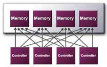
LMA II - new memory architecture It was thanks to improvements in the memory architecture that the GeForce4 Ti showed such a strong lead over the GeForce3.
In GeForce3/GeForce4, the memory controller was divided into four independent controllers, each of which uses a dedicated 32-bit DDR bus. All memory requests were shared between these controllers.
In LMA II, almost every component has been improved. You can pay attention to four caches. But caching is exclusive to GeForce, as the Radeon 8500 also had similar caches. In general, caching in graphics chips received much less attention than caches in processors, since their size was not so large. The reason for this is clear: graphics chips were then slower than memory buses, while central processors were 2-16 times faster, so the cache played a much more important role there.
Crossbar memory controller The
GeForce3 already had this controller, allowing for 64-bit, 128-bit, and normal 256-bit transfers, greatly improving throughput. In LMA II, nVidia improved the load balancing algorithms for different memory sections and modernized the priority scheme.
Visibility Subsystem - Overlapped Pixel Rejection
This technology already existed in the GeForce3, but it has been improved in the NV25 for more accurate pixel culling using less memory bandwidth. Rejection was then carried out using a special cache on the chip, which made it possible to reduce the access to the external memory of the video card. According to Anandtech's research, the GeForce4 was 25% better at rejecting pixels than the GeForce3 at the same clock speed.
Lossless Z-Buffer Compression
Again, this feature existed in the GeForce3, but thanks to the new compression algorithm, LMA II was more likely to achieve successful 4:1 compression.
Vertex Cache
Stores vertices after they have been sent over AGP. The cache improved the use of AGP, as it allowed us to avoid passing identical vertices (for example, if the primitives had common boundaries).
Primitive Cache
Accumulated primitives after they were processed (after the vertex shader) into fundamental primitives to be passed to the triangle setup module.
Dual Texture Cache
Already existed on the GeForce3. The new algorithms worked better when using multitexturing or high quality filtering. Thanks to this, GeForce4 Ti has significantly improved performance when applying 3-4 textures.
Pixel cache
The cache was used at the end of the rendering pipeline for accumulation, very similar to the feature in Intel/AMD processors. The cache accumulated a certain number of pixels and then in batch mode wrote them into memory.
Automatic pre-charge
Before reading from the memory bank, it must be pre-charged, which leads to delays. The GeForce4 Ti could proactively charge using a special prediction algorithm.
Fast Z-clear (Z-clear)
This feature has been known for some time and used in other chips. Fast Z-clearing was first used on an ATi Radeon chip. It simply set a flag for a certain section of the frame buffer, so that instead of filling this section with zeros, you could just set a flag, which saved memory bandwidth.

Specifications NVIDIA GeForce 4 Ti 4200
| Name | GeForce 4 Ti 4200 |
| Core | NV25 |
| Process technology (µm) | 0.15 |
| Transistors (million) | 63 |
| Core frequency | 250 |
| Memory frequency (DDR) | 222 (444) |
| Bus and memory type | DDR-128bit |
| Bandwidth (Gb/s) | 7.1 |
| Pixel pipelines | 4 |
| TMU per conveyor | 2 |
| textures per clock | 8 |
| textures per pass | 4 |
| Vertex conveyors | 2 |
| Pixel Shaders | 1.3 |
| Vertex Shaders | 1.1 |
| Fill Rate (Mpix/s) | 1000 |
| Fill Rate (Mtex/s) | 2000 |
| DirectX | 8.0 |
| Anti-Aliasing (Max) | MS - 4x |
| Anisotropic Filtering (Max) | 8x |
| Memory | 64 / 128 MB |
| Interface | AGP4x |
| RAMDAC | 2x350 MHz |
The GeForce4 Ti 4200 is a lighter version of the GeForce4 Ti 4600 or 4400 that had a lower clock speed but was much cheaper.
In many ways, the GeForce4 Ti 4200 can be considered a potential "gravedigger" of the GeForce3 Ti 500 line. not in favor of the latter. Therefore, NVIDIA delayed the release of the Ti 4200 until a later date, until there was a significant decline in sales in the GeForce3 line.
Mafia