


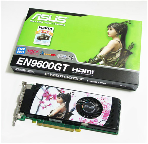
GeForce 9600 GT
In the case of G94, we see an elementary reduction - 4 shader units, each of which contains 16 stream processors (Streaming Processor) and 8 texture units (TMU). In total, 64 stream processors and 32 texture units are obtained. All G94 processors, as in previous chips, operate at higher clock frequencies relative to the GPU. In particular, for the 9600 GT it is 1650 MHz. Finally, we note the blocks for writing to the frame buffer (ROP), which in this case are 4 (in the diagram, blue blocks next to the L2 cache). In the work and concept of building stream processors (SP), NVIDIA has not made any amendments since the time of the G84 chips.
For every four stream processors, there are two TA texture addressers and two TF texture filter modules. Therefore, now each texture unit, due to the increase in the number of calculated texture addresses, will be able to process twice as many samples as, for example, in the G80. Each shader unit has its own L1 cache. It can store not only textures, but also, due to the unification of the blocks themselves, various kinds of data. All stream processors (SPs) on which the G94 architecture is based are scalar. Why not vector? The reason lies in the fact that based on the research of shader programs by NVIDIA developers, it was found out that the vector architecture uses computing resources quite uneconomically when complex instructions are being processed - for example, scalar and vector at the same time (generally speaking, scalar calculations on vector processors are performed very inefficiently). In light of the recent trend towards an increasing transition from vector to scalar computing, the strategy of NVIDIA developers, perhaps, becomes clear. Well, what to do with the vector program code? Everything is very simple: they are converted into scalar operations directly by the G94 chip itself. As already mentioned, the GeForce 9600 has 4 frame buffer write units (ROP). They have not undergone any changes regarding the G92 architecture and support the following anti-aliasing methods: multisampling, supersampling and adaptive anti-aliasing. In light of the recent trend towards an increasing transition from vector to scalar computing, the strategy of NVIDIA developers, perhaps, becomes clear. Well, what to do with the vector program code? Everything is very simple: they are converted into scalar operations directly by the G94 chip itself. As already mentioned, the GeForce 9600 has 4 frame buffer write units (ROP). They have not undergone any changes regarding the G92 architecture and support the following anti-aliasing methods: multisampling, supersampling and adaptive anti-aliasing. In light of the recent trend towards an increasing transition from vector to scalar computing, the strategy of NVIDIA developers, perhaps, becomes clear. Well, what to do with the vector program code? Everything is very simple: they are converted into scalar operations directly by the G94 chip itself. As already mentioned, the GeForce 9600 has 4 frame buffer write units (ROP). They have not undergone any changes regarding the G92 architecture and support the following anti-aliasing methods: multisampling, supersampling and adaptive anti-aliasing. the GeForce 9600 has 4 framebuffer writes (ROPs). They have not undergone any changes regarding the G92 architecture and support the following anti-aliasing methods: multisampling, supersampling and adaptive anti-aliasing. the GeForce 9600 has 4 framebuffer writes (ROPs). They have not undergone any changes regarding the G92 architecture and support the following anti-aliasing methods: multisampling, supersampling and adaptive anti-aliasing.
Specifications NVIDIA GeForce 9600 GT
| Name | GeForce 9600 GT |
| Core | G94 (D9P) |
| Process technology (µm) | 0.065 |
| Transistors (million) | 505 |
| Core frequency | 650 |
| Memory frequency (DDR) | 900 |
| Bus and memory type | GDDR3 256-bit |
| Bandwidth (Gb/s) | 57.60 |
| Unified shader blocks | 64 |
| Frequency of unified shader units | 1625 |
| TMU per conveyor | 32 |
| ROP | 16 |
| Shader Model | 4.0 |
| Fill Rate (Mpix/s) | 10400 |
| Fill Rate (Mtex/s) | 20800 |
| DirectX | 10.0 |
| Memory | 512/1024 |
| Interface | PCI-E 2.0 |