


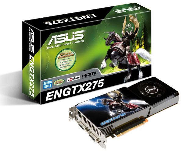
GeForce GTX 275
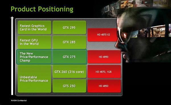
There was a need for an inexpensive accelerator that could confidently compete with the HD 4890. NVIDIA did not invent something new, but slightly changed the GTX 285, resulting in the GTX 275.
There are few differences from the flagship of the line of single-chip video cards. The memory bus went under the knife - instead of 512 bits in the GTX 275, it is 448 (the same as in the GTX 260), controllers that have become "unnecessary" and part of the ROP are disabled, and, of course, the number and total volume of GDDR3 chips have slightly decreased soldered on the board.
Specifications NVIDIA GeForce GTX 275
| Name | GeForce GTX 275 |
| Core | GT200b |
| Process technology (µm) | 0.055 |
| Transistors (million) | 1400 |
| Core frequency | 633 |
| Memory frequency (DDR) | 1134 (2268) |
| Bus and memory type | GDDR3 448-bit |
| Bandwidth (Gb/s) | 127.008 |
| Unified shader blocks | 240 |
| Frequency of unified shader units | 1404 |
| TMU per conveyor | 80 |
| ROP | 28 |
| Shader Model | 4.0 |
| Fill Rate (Mpix/s) | 17724 |
| Fill Rate (Mtex/s) | 50640 |
| DirectX | 10.0 |
| Memory | 896.1792 |
| Interface | PCIe 2.0 |
With the task set - to create a worthy rival to the Radeon HD 4890 - NVIDIA has successfully coped. In fact, the Californians have taken a number of measures to reduce the price of the GTX 285 by $70-90 without harm to themselves. As for the lost megabytes of video memory and damaged bits of the memory bus, they can be easily compensated for by overclocking - even with a standard cooling system, the video chip can easily be overclocked to 720-750 MHz. Of course, you can't increase the amount of memory by raising the clock frequencies, but the missing 128 MB is almost never decisive.