


GeForce GTX 280
Moreover, each TPC module consists of an array of streaming multiprocessors (SM, Streaming Multiprocessors), and each SM contains eight processor cores, also called stream processors (SP, Streaming Processor), or thread processors (TP, Thread Processor). Each SM also includes texture filtering processors for graphics mode, also used for various filtering operations in compute mode.
Below is a block diagram of the GeForce 280 GTX in traditional graphics mode.
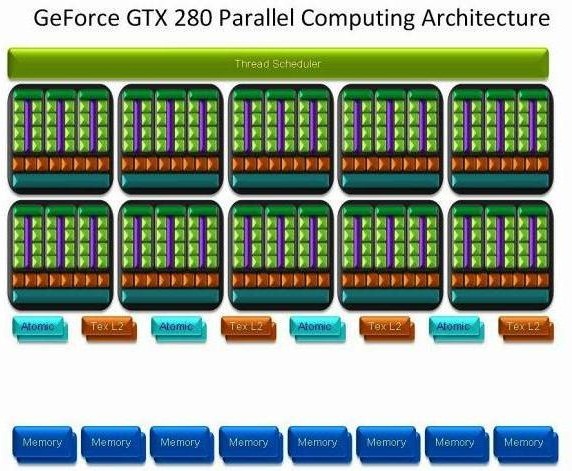
By switching to compute mode, the hardware thread manager (above) manages the TPC threads.
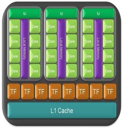
Closer look at the TPC cluster: shared memory per SM; each SM processor core can share data among other SM cores via distributed memory, without the need to access an external memory subsystem.
Thus, NVIDIA's unified shader and computer architecture uses two completely different computational models: for TPC operation, MIMD (multiple instruction, multiple data) is used, for SM computations - SIMT (single instruction, multiple thread), advanced version, SIMD (single instruction, multiple data).
In terms of general characteristics, compared to previous generations of chips, the GeForce GTX 200 family has the following advantages:
Ability to process 3x more data streams per unit time
New instruction scheduler design with 20% more texture processing efficiency
512-bit memory interface (previous gen 384 bits)
Optimized z-sampling and compression process for better performance at high screen resolutions
Architectural enhancements to increase shadow processing performance
Full-speed framebuffer blending (vs. half-speed on the 8800 GTX)
Doubled instruction buffer for improved compute performance
Doubled number of registers for faster processing of long and complex shaders
Double-precision floating-point data according to IEEE 754R version
10-bit color space hardware support (DisplayPort only)
Here is a list of the main characteristics of the new chips:
NVIDIA PhysX support
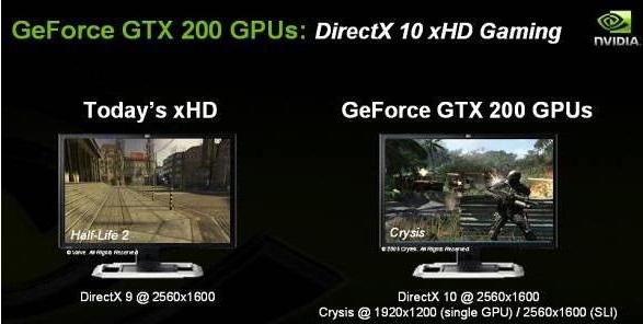
Microsoft DirectX 10, Shader Model 4.0
support NVIDIA CUDA technology
support PCI Express 2.0 bus support
GigaThread technology support
NVIDIA Lumenex engine
128-bit floating point (HDR)
OpenGL 2.1
support Dual Dual-link DVI
support NVIDIA PureVideo HD technology support
Support for NVIDIA HybridPower technology
Separately, it is noted that DirectX 10.1 is not supported by the GeForce GTX 200 family. The reason is the fact that when developing chips of a new family, after consultations with partners, it was customary to focus not on supporting DirectX 10.1, which is still in little demand, but on improving the architecture and performance of the chips.
Based on a package of physics algorithms, the implementation of NVIDIA PhysX technology is a powerful real-time physics engine. Currently, PhysX support is implemented in more than 150 games. Combined with a powerful GPU, the PhysX engine provides a significant increase in physical processing power, especially in such areas as creating dust and debris explosions, characters with complex facial expressions, new weapons with fantastic effects, realistically worn or torn fabrics, fog and smoke with dynamic flow around objects.
Many developers and game developers have been striving to implement physical effects in games for a long time. Every year this direction becomes more and more relevant. In modern games, the interaction of objects with the environment is carried out by the forces of two engines that have gained the greatest popularity - Havok and PhysX.
Havok is the oldest engine on which many games are written for PC and consoles. Back in 2006, the then independent ATI demonstrated the acceleration of physical effects by the forces of Radeon X1900XT video cards. However, Havok was later bought by Intel, which stated that the physical effects would be calculated by this engine using processors.
PhysX was developed by AGEIA, which implemented "physics" with accelerators of its own design. But it so happened that, despite the great popularity of this engine among game developers, the implementation of physical effects in games by specialized accelerators turned out to be very controversial.
And last year, NVIDIA bought AGEIA PhysX. A statement was made that through driver optimization, the PhysX engine will be adapted to the use of GeForce 8800GT and higher video cards.
Another important innovation is the new energy saving modes. Using a precision 65 nm process technology and new circuit solutions, more flexible and dynamic power control has been achieved. Thus, the consumption of the GeForce GTX 200 family of graphics chips in standby mode or in 2D mode is about 25 W; when playing a Blu-ray DVD movie - about 35 W; at full 3D load TDP does not exceed 236 watts. The GeForce GTX 200 graphics chip can be completely disabled due to the support of HybridPower technology with motherboards based on nForce HybridPower chipsets with integrated graphics (for example, nForce 780a or 790i), while the low-intensity graphics stream is simply processed by the GPU integrated into the motherboard. Besides,
The user can configure a system based on two or three video cards of the GeForce GTX 200 family in SLI mode when using motherboards based on the corresponding nForce chipsets. In the traditional Standard SLI mode (with two video cards), about 60-90% performance increase in games is declared; in 3-way SLI mode - the maximum number of frames per second at maximum screen resolutions.
As part of the announcement of the new GeForce GTX 200 family of GPUs, NVIDIA offers a completely new look at the role of the CPU and GPU in the modern balanced desktop system. Such an optimized PC, based on the concept of heterogeneous computing (that is, computing a stream of heterogeneous heterogeneous tasks), according to NVIDIA experts, has a much more balanced architecture and significantly greater computing potential. This refers to the combination of a relatively moderate performance CPU with the most powerful graphics or even SLI system, which allows peak performance in the most demanding games, 3D and media applications.
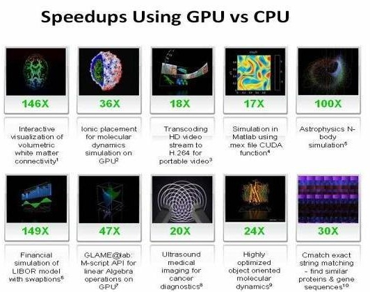
On the other hand, intensive computing with the help of modern graphics cards is not new for a long time, but it is with the advent of the GeForce GTX 200 family of graphics processors that NVIDIA expects a significant increase in interest in CUDA technology.
CUDA (Compute Unified Device Architecture) is a computing architecture aimed at solving complex problems in consumer, business and technical fields - in any data-intensive applications using NVIDIA GPUs. From the point of view of CUDA technology, the new GeForce GTX 280 graphics chip is nothing more than a powerful multi-core (hundreds of cores!) Processor for parallel computing.
As mentioned above, the graphics core of the GeForce GTX 200 family can be thought of as a chip that supports graphics and computing modes. In one of these modes - "computing", the same GeForce GTX 280 turns into a programmable multiprocessor with 240 cores and 1 GB of dedicated memory - a sort of dedicated supercomputer with teraflop performance, which significantly increases the performance of applications that parallelize data well, for example , video encoding, scientific computing, etc.
The GeForce 8 and 9 families of graphics processors were the first on the market to support CUDA technology, with more than 70 million units sold, and interest in the CUDA project is constantly growing. Learn more about the project and download the files you need to get started here. As an example, the screenshots below show examples of computational performance gains obtained by independent users of CUDA technology.
Compared to the previous leader GeForce 8800 GTX, the new flagship GeForce GTX 280 has 1.88 times the number of processor cores; capable of processing about 2.5 more threads per chip; has twice the size of file registers and support for double-precision floating-point calculations; supports 1GB memory with 512-bit interface; equipped with a more efficient command dispatcher and improved communication capabilities between chip elements; improved Z-buffer and compression module, support for 10-bit color palette, etc.
For the first time, a new generation of GeForce GTX 200 chips is initially positioned not only as a powerful 3D graphics accelerator, but also as a serious computer solution for parallel computing.
Specifications NVIDIA GeForce GTX 280
| Name | GeForce GTX 280 |
| Core | GT200 (D10U-30) |
| Process technology (µm) | 0.065 |
| Transistors (million) | 1400 |
| Core frequency | 602 |
| Memory frequency (DDR) | 1107 |
| Bus and memory type | GDDR3 512-bit |
| Bandwidth (Gb/s) | 141.67 |
| Unified shader blocks | 240 |
| Frequency of unified shader units | 1296 |
| TMU per conveyor | 80 |
| ROP | 32 |
| Shader Model | 4.0 |
| Fill Rate (Mtex/s) | 48160 |
| DirectX | 10 |
| Interface | PCIe 2.0 |
The revolution did not happen, the new GPU GT200 and the video card GeForce 280GTX (285GTX , 295GTX) tested today are a further development of the unified shader architecture from NVIDIA. The new GPU contains more functional blocks than its predecessors, which gives it the right to be called the most powerful GPU to date.