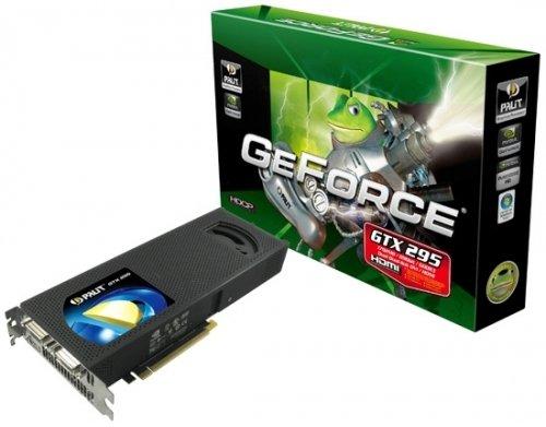
GeForce GTX 295
Despite the fact that the GeForce GTX 295 and the Radeon HD 4870 X2 are conceptually identical, they differ significantly in terms of design. This is due to the peculiarities of the graphics controllers used in them.
The RV770 graphics processor found in the Radeon HD 4800 series supports a 256-bit memory bus, while NVIDIA's GT200 processor supports a 512-bit one. In addition, the external interface controller is integrated in the RV770, while in the GT200 it is made as a separate microcircuit. When creating a dual-processor video card, AMD managed with one printed circuit board with two 256-bit buses for connecting two 3D chips to the memory. It also had a PCI Express bus switch, two 1024 MB GDDR5 chipsets, and power circuits. Therefore, the AMD dual-processor video card differs slightly in technological complexity from the competitor's single-processor models, on which, in addition to the graphics controller itself, a second chip responsible for external interfaces is installed.
As we have already said, architecturally GeForce GTX 295 does not differ from its competitor. From the point of view of the system, these are two video cards with PCI Express interface, each with its own array of local memory and a set of output ports. Only their connection was made not by means of system logic (motherboard chipset), but with the help of an additional PCI Express switch. Video cards operate in SLI mode, rendering frames one by one and writing them to the output video buffer of one of them - the one to which the monitor is connected.
Structurally, the GeForce GTX 295 is made differently than the Radeon HD 4870 X2.
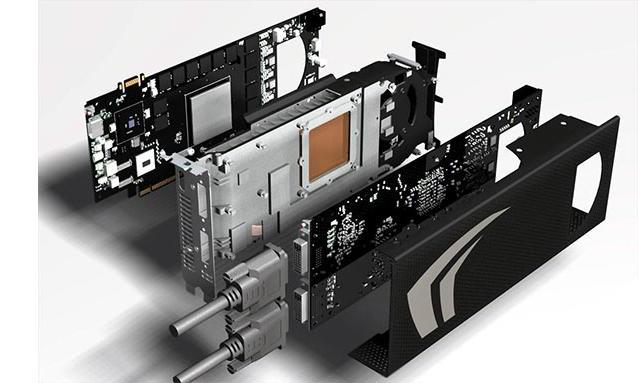
It actually consists of two printed circuit boards, only turned by the front sides to each other. On one board there is the first GT200 graphics chip, an NVIO chip (responsible for external interfaces) and an nForce 200 bridge (PCI Express switch), on the other - the second GT200 with its own NVIO chip.
But recently, the Californians still switched to the new design of their flagship GeForce GTX 295, which now uses only one printed circuit board. According to the design of the GeForce GTX 295 Rev. B is fundamentally different from its predecessor, both due to the layout of the elements on the same board, and due to the 85 mm fan located in the center, the air from which exits both outside the system unit and inward through the end of the card. Something similar was used back in the days of the GeForce 7900 GTX.
The GTX 295 uses a version of the GT200 chip which, like the GTX 260 cards, does not have all feature units enabled. However, the good news is that the number of feature units included is even greater than the latest GTX 260 cards with 216 cores.
All texture and shader units in this version of the GT200 GPU work as they do in the GTX 280 chip. The only real downside is the number of ROPs (and therefore the memory bus width). Like the GTX 260 cards, each GT200 chip in the GTX 295 has 28 ROPs and a 448-bit memory interface mapped to 896MB of RAM.
Specifications NVIDIA GeForce GTX 295
| Name | GeForce GTX 295 |
| Core | GT200b x 2 |
| Process technology (µm) | 0.055 |
| Transistors (million) | 1400 |
| Core frequency | 576 |
| Memory frequency (DDR) | 999 (1998) |
| Bus and memory type | GDDR3 448-bit x 2 |
| Bandwidth (Gb/s) | 223.776 |
| Unified shader blocks | 240x2 |
| Frequency of unified shader units | 1242 |
| TMU per conveyor | 80x2 |
| ROP | 32x2 |
| Shader Model | 4.0 |
| Fill Rate (Mpix/s) | 32256 |
| Fill Rate (Mtex/s) | 92160 |
| DirectX | 10.0 |
| Memory | 1792 |
| Interface | PCIe 2.0 |
This product from Nvidia is currently the fastest graphics card on the market.
Grand Theft Auto IV