


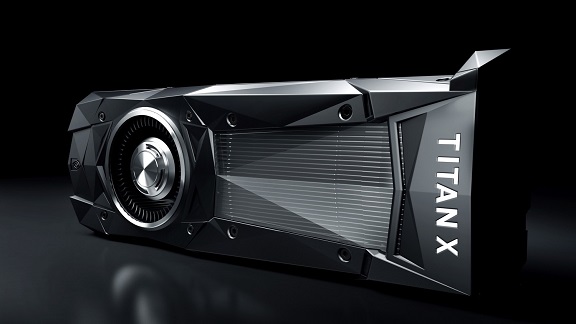
NVIDIA TITAN X
The new TITAN X, which became the first device based on the GP102 processor, was positioned primarily as a professional-grade accelerator that is designed for research and commercial applications related to deep learning.
This GPU is conceived as an alternative to the supercomputer GP100, which is not inferior to the latter in the functions of rendering 3D graphics and FP32 calculations. At the same time, the creators of the GP102 have reduced all components that do not correspond to the purpose of the product.

For example, a single SM (Streaming Multiprocessor - a block that combines CUDA cores along with texture mapping units, schedulers, dispatchers and local memory segments) in GP100 contains 64 CUDA cores for FP32 operations, while SM in GP102 has in this respect configuration inherited from Maxwell: 128 CUDA cores. The finer distribution of CUDA cores in the GP100 allows the processor to simultaneously execute more instruction streams (and also thread groups - warps - and warp blocks), and the total amount of storage types inside the SM, such as shared memory (shared memory) and register file, in in terms of the entire GPU has increased compared to the Maxwell architecture.
Further, in GP100, for every 64 CUDA cores for FP32 operations, there are 32 cores for FP64, while the SM in GP102 has a configuration inherited from Maxwell in this regard: 128 CUDA cores for FP32 and 4 for FP64. Hence the truncated double precision performance of the GP102.
Finally, the GP100 carries a larger L2 cache: 4096 KB versus 3072 KB in the GP102. And of course, the GP102 lacks an NVLINK bus controller, and the HBM2 memory controllers (with a total bus width of 4096 bits) are replaced by GDDR5X SDRAM controllers. 12 of these 32-bit controllers provide a common 384-bit memory access bus.
The GP102 die, manufactured using TSMC's 16nm FinFET process technology, contains 12 billion transistors in an area of 471mm2. For comparison: the characteristics of the GP100 are 15.3 billion transistors and 610 mm2. This is a very significant difference. In addition, if TSMC has not increased the size of the photomask for the 16nm process compared to 28nm, then the GP100 is almost exhausted, while the lightweight architecture of the GP102 will allow NVIDIA to create a larger core for the broad consumer market in the future, using the same production line. (Which, however, is unlikely to happen unless developers rethink their TDP standards for top models).
NVIDIA TITAN X Specifications
|
|
||||||
|
Chip
|
||||||
|
Frequencies
|
||||||
|
Memory
|
||||||
|
Interface and TDP
|
The graphics processor of the novelty operates at higher frequencies (1417/1531 MHz) than in the Tesla P100 (up to 1328/1480 MHz in the supercomputer version and up to 1300 MHz in the form factor of the PCI-Express board). Still, the frequencies of the "Titan" are quite conservative compared to the characteristics of the GeForce GTX 1080 (1607/1733 MHz). As we'll see in the overclocking experiments, the limiting factor was the device's power consumption, which NVIDIA set at its familiar 250W. NVIDIA Titan X has 3,584 stream processors at its disposal.
TITAN X is equipped with 12GB GDDR5X SDRAM with a bandwidth of 10Gbps per pin. The 384-bit bus provides data transfer at a speed of 480 GB / s: in this indicator, TITAN X is only slightly inferior to the current record holder - Radeon R9 Fury X, as well as other AMD products based on Fiji GPUs (512 GB / s).