


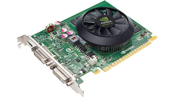
GEFORCE GT 640
GEFORCE GT 640 is the first model based on Kepler architecture, which used GK107 instead of GK104 GPU. The area of the GK107 chip, containing 1.3 billion transistors, is 118 mm2, which is significantly less than that of the GK104 with 294 mm2. Essentially, the GK107 chip on the GeForce GT 640 uses a quarter of the shader resources of the full featured GK104 GPU. The 384 CUDA cores are divided into two SMX units, each containing 16 texturing units (32 in total). The core frequency of the new chip is 900 MHz. The GeForce GT 640 cannot dynamically upclock when thermal headroom allows because the card lacks the GPU Boost feature found on cards with the GK104.
The GPU core consists of two groups of ROPs, each capable of outputting eight 32-bit pixels per clock, for a total of 16. The two 64-bit memory buses add up to 128-bits. 2 GB DDR3 memory runs at 891 MHz, resulting in a memory bandwidth of up to 28.5 GB/s.
Specifications GeForce GT 640
| Name | GeForce GT 640 |
| Core | GK107 |
| Process technology (µm) | 0.028 |
| Transistors (million) | 1300 |
| Core frequency | 900 |
| Memory frequency (DDR) | 891 (1782) |
| Bus and memory type | 128-bit GDDR3 |
| Bandwidth (Gb/s) | 28.5 |
| Unified shader blocks | 384 |
| Frequency of unified shader units | 900 |
| TMU per conveyor | 32 |
| ROP | 16 |
| DirectX | 11.1 |
| Memory | 2048 |
| Interface | PCI-E3.0 |
The power consumption of the card, according to Nvidia, is 65W, which does not exceed the limit of the 16-lane PCI Express slot, which can power loads up to 75W.