


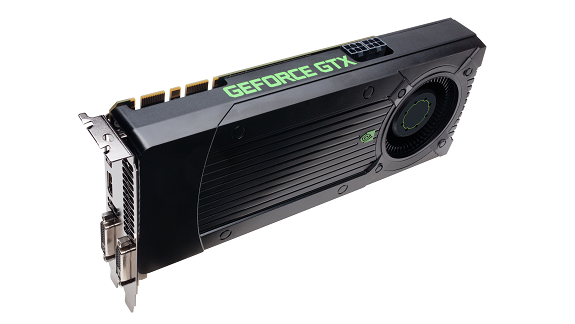
GEFORCE GTX 660 Ti
Compared to previous NVIDIA cards that occupied the niche of the GeForce GTX 660 Ti, it was in a unique position. Both the GeForce GTX 460 and GTX 560 Ti were based on GF114 chips, while the GTX 480 and GTX 580 used GF100 and GF110 processors with a significantly larger number of computing units. This time, the top adapters of the Kepler family are equipped with second-order processors, GK104, and the "big Kepler" - GK110 - is still looming somewhere on the horizon. The third-order GPU, GK107, which formed the basis of the GeForce GT 640, is too weak to form a line of adapters in the High-Middle End category. Therefore, they decided to equip the GTX 660 Ti with the rest of the GK104 chips from the production of the GTX 670 and GTX 680. And, as you will see, there are quite a few left.
For starters, GTX 660 Ti cards are built on GTX 670 circuit boards according to the reference specifications. Some manufacturers have used this trick in the past with original design GTX 560 Ti cards that were factory overclocked. The GPU and memory clocks of the GTX 660 Ti and GTX 670 are also the same: 915 MHz for the base clock and 980 for the Boost Clock. Like the older cards in the family, the GTX 660 Ti uses the GPU Boost feature, which dynamically increases the processor frequency if the current power consumption allows it, while remaining within the standard TDP.
Biggest surprise: The GTX 660 Ti has the same number of active streaming multiprocessors (SMX) and CUDA cores as the GTX 670 (7 SMX and 1344 cores). The number of texture units also remained unchanged. What has been damaged? There are 24 ROPs left out of 32 and three out of four 64-bit memory controllers, due to which the memory bus width has been reduced from 256 to 192 bits. The L2 cache is 384KB versus 512 for the GTX 670 and GTX 680.
Like other Kepler cards, the GTX 660 Ti supports all the innovations of this architecture: the PCI-E 3.0 bus, DirectX 11.1 graphics features, and so on. On the other hand, the GX 660 Ti also inherited a characteristic weakness of all products based on the GK104 chip: performance in non-graphical calculations with double precision (FP64) is 1/24 of that of FP32. For comparison, the GF110 runs at 1/8 FP32, while the AMD Tahiti processor in the Radeon HD 7950 and HD 7970 runs at 1/4 FP32.
Specifications GeForce GTX 660 Ti
| Name | GeForce GTX 660 Ti |
| Core | GK104 |
| Process technology (µm) | 0.028 |
| Transistors (million) | 3540 |
| Core frequency | 915 (Boost Clock 980) |
| Memory frequency (DDR) | 3004 (6008) |
| Bus and memory type | 192-bit GDDR5 |
| Bandwidth (Gb/s) | 144.192 |
| Unified shader blocks | 1344 |
| Frequency of unified shader units | 915 (Boost Clock 980) |
| TMU per conveyor | 112 |
| ROP | 24 |
| DirectX | 11.1 |
| Memory | 2048 |
| Interface | PCI-E3.0 |
Having rid the GeForce GTX 660 Ti of part of the computing units, NVIDIA reduced the TDP of the card by another 20 W compared to the power consumption of the GTX 670 - up to 150 W. Of the current and previous generation AMD cards, the Radeon HD 6790 (150 W), HD 7850 (130 W) and HD 7870 (175 W) are the closest in terms of gluttony. Compared to NVIDIA GeForce 500 series cards, there is also progress in this parameter. The GTX 560 has the same TDP as the GTX 660 Ti, while the GTX 560 Ti already consumes 170 watts.