


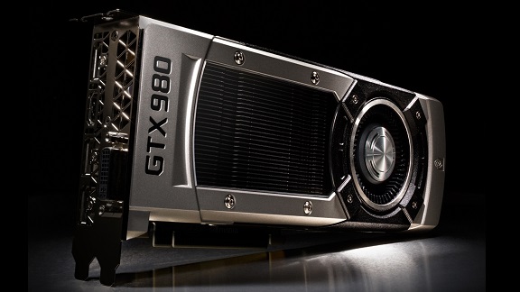
GeForce GTX 980
Maxwell is the first fruit of NVIDIA's strategy to design new GPU architectures with mobile and ultra-mobile first and foremost, with power efficiency at the forefront.
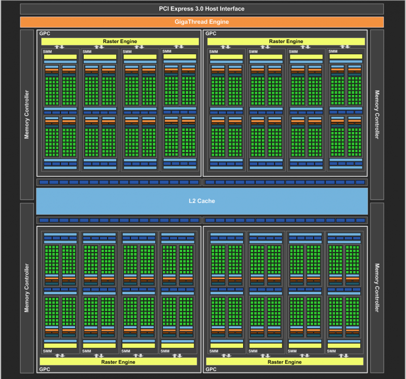
All computational logic is concentrated in structures called the Graphics Processing Cluster (GPC), of which there are four in the GM204. Outside the GPC is the entire back-end of the processor in the form of ROP blocks and several 64-bit memory controllers, as well as the Giga Thread Engine, which performs the functions of context change, simultaneous execution of kernels and distribution of load flows between the GPC.
Maxwell's key innovation is that execution units are no longer equally addressable by any scheduler. Each scheduler now has at its disposal a fixed part of the resources: 32 CUDA cores, 8 Load / Store blocks and SFU (Special Function Units, performing, for example, trigonometric operations). Only texture units and CUDA cores compatible with FP64 computing are still shared resources.
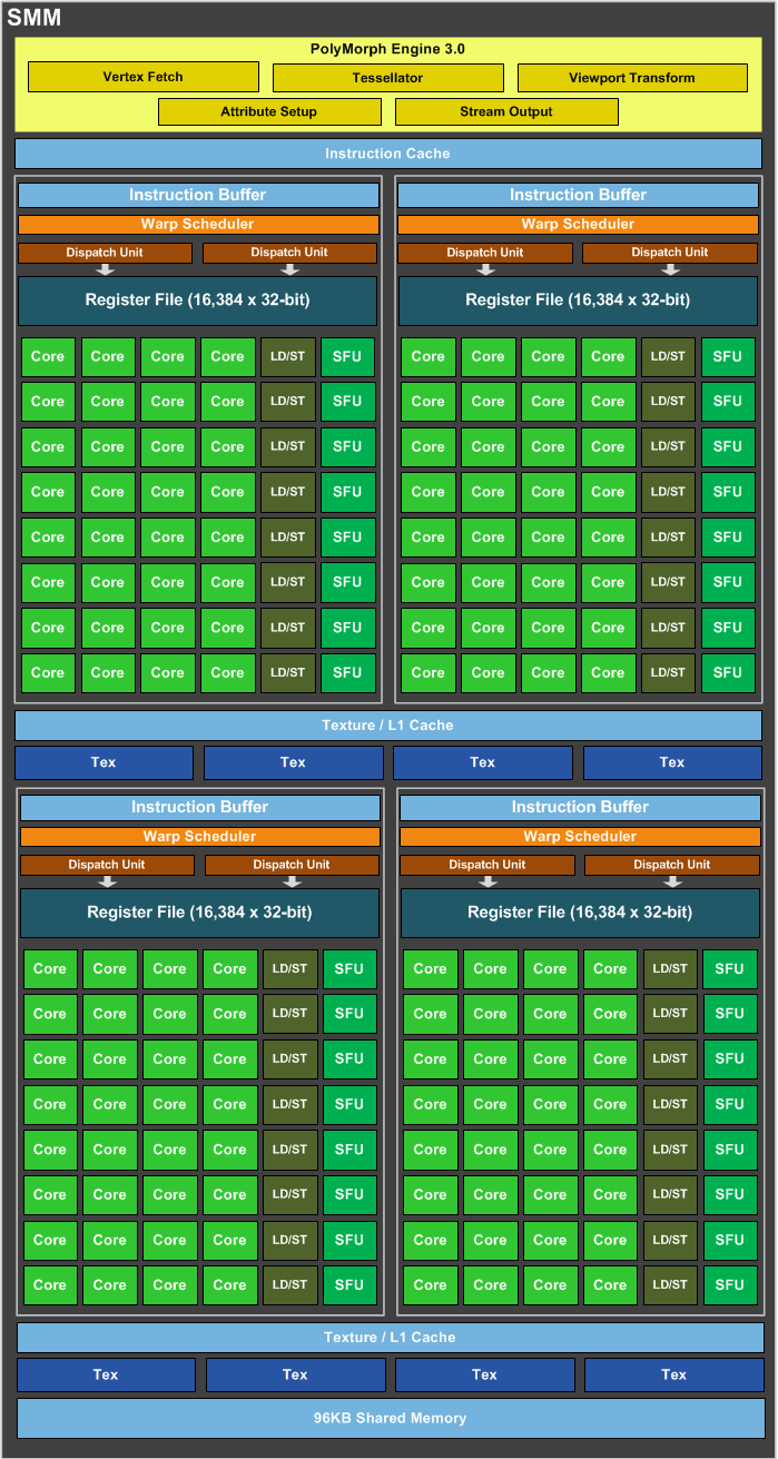
Maxwell is based on power optimizations introduced in the Kepler architecture. After the Fermi architecture, NVIDIA abandoned dynamic schedulers inside the GPU, shifting all the work of scheduling out-of-order execution of instructions to the compiler as part of the driver.
about the number of computing units, the chip is an intermediate option between GK104 and GK110. It doesn't have as many CUDA cores as the GK110. But, taking into account the different architecture, it is impossible to directly compare the chips based on Kepler and Maxwell in terms of the number of execution units.
Finally, the GM204 has more ROPs than the top Kepler, 64 versus 48. This will clearly benefit the 4K resolution video adapter, as shown by the AMD Hawaii GPU, which also carries 64 ROPs. However, to realize this potentially high pixel fill rate, sufficient DRAM bandwidth is required.
Meanwhile, the memory bus configuration of the adapters on the GM204 is the same as that of the GeForce GTX 770: 256 bits and an effective frequency of 7 GHz, while the GK110 and Hawaii use 384-bit and 512-bit buses, respectively. The creators of the GM204 had to take measures to save the bandwidth of the interface, which, in addition to the increased L2 cache, consists in a new color compression algorithm. This is the third version of the algorithm, first introduced in the NV40 chip, which allows data to be compressed at a ratio of up to 8:1 without information loss.
Specifications GeForce GTX 980
|
|
||||||
|
Chip
|
||||||
|
Frequencies
|
||||||
|
Memory
|
||||||
|
Interface and TDP
|
The GeForce GTX 980 is based on the GM204 GPU, which is manufactured using a 28nm process technology and contains 5.2 billion transistors. 2.048 stream processors operate at a base clock speed of 1.126 MHz. In Boost mode, the minimum frequency is 1.216 MHz. 4.096 MB of GDDR5 memory are connected via a 256-bit interface and operate at 1.750 MHz. 2,048 stream processors make up 16 Maxwell multiprocessors, each containing 128 ALUs. We also get 128 texture units and 64 raster operation pipelines.