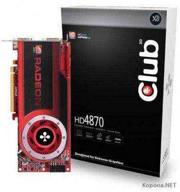
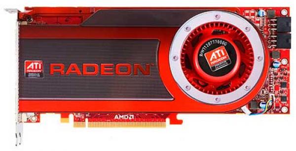
Radeon HD 4870
If in the case of RV670 (Radeon HD 38x0) the legitimacy of assigning the next generation number could be questioned, since this GPU differed little from the core of the previous generation, R600 (Radeon HD 2900), then with RV770 such doubts do not arise - this is really a new product, albeit inheriting most of the features of its predecessors. The new family was named ATI Radeon HD 4800, and the naming scheme for different graphics card models, first used by ATI in the ATI Radeon HD 3800 family, is retained: the first digit means the generation of the graphics architecture, the second - the family, and the last two - the model of a particular video adapter.
The RV770 core consists of 956 million transistors, which is quite impressive at first glance, however, it is not an absolute record in the industry; The palm in this area belongs to Nvidia with its GT200 chip, which has 1.4 billion transistors. The superiority can be called doubtful, since ATI's competitor uses a less advanced 65-nm process technology, which, given the huge area and complexity of such a core, automatically means a smaller number of cores on the substrate and a lower yield, and, consequently, a significantly higher production cost, however, such an approach is a typical Nvidia tactic in recent years. Cards based on the GT200 are unlikely to become cheap over time, unlike the new ATI solutions using the RV770. Thus, the strategy chosen by ATI Technologies, at first glance, fully justifies itself.
It should be noted that the GPU frequencies were noticeably lowered compared to cards based on the previous generation GPU, RV670, which can be explained by the significantly increased complexity of the new core. Given the increased processing and texturing power, this should not be any problem. Another interesting detail that deserves attention: the use of fast GDDR5 memory in the older ATI Radeon HD 4800 model made it possible to achieve high bandwidth without resorting to expanding the external access bus, as ATI did last year and Nvidia is doing now. An increase in the memory bus width over the traditional 256 bits leads to a significant complication of the printed circuit board, and, consequently, to its rise in price. Of course, GDDR5 memory is more expensive than the widespread GDDR3, but apparently
It is clearly seen that the topology of the memory access subsystem as a whole has been preserved, although now it cannot be called ring: almost every memory controller is connected by a bidirectional interface to another, however, the "ring" itself is no longer closed. The memory access interface is still located around the perimeter of the crystal, and next to it are the functional blocks that are most critical to throughput:
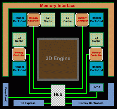
At the same time, a switch appeared in the core that interconnects blocks that are less demanding on bandwidth - the PCI Express bus interface, the CrossFireX interface, the UVD2 video processor, display controllers, etc. The memory subsystem resource utilization efficiency in previous generations of ATI Radeon HD already reached 85% according to ATI, and the RV770 topology optimization made it possible to bring it almost to the maximum. Together with the possibility of using fast GDDR5 memory, this eliminated the need for developers to use an external bus with a capacity of more than 256 bits, which had a positive effect on the simplicity of the design of ATI Radeon HD 4800 printed circuit boards.
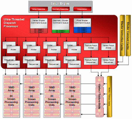
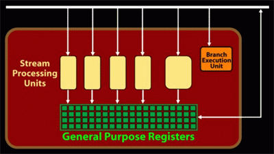
A key part of any graphics core with a modern architecture is the task manager block, which is entrusted with the work of distributing the available processor resources in such a way that all its parts are maximally loaded, and, therefore, the performance tends to be as high as possible.
The task manager block first appeared as part of the ATI Radeon X1000 family, where it could manage 512 code branches of 16 pixels each. The second version of the task distribution processor was introduced in the ATI Radeon HD 2000. The new handler not only could process more code branches, but also do it more accurately and efficiently - the minimum branch size was reduced from 16 to 5 pixels.
The computing part of the R600 and RV670 consisted of 64 universal modules, each of which included five ALUs, a flow control unit, and an array of general purpose registers. Four out of five ALUs were quite simple devices capable of executing one FP MAD instruction per cycle, and the fourth was complex, able to work with complex SIN, COS, LOG, EXP, etc. instructions. In fact, each computing module was a processor with a five-stage pipeline.
In theory, such an organization made it possible to talk about the presence of 320 actuators, but in fact, this was true only for the case of a full load of all 64 pipelines, which in practice was far from always provided: in three-dimensional applications, many operations depend on the results of previous operations, therefore, consistent pipeline operation is not easy to achieve. This requires significant optimizations for a specific application at the level of Catalyst drivers, but it is not always possible to get access to the software "stuffing" of the game, at least until its official release.
As a result, in practice, it often turned out that only one ALU in each computing module was doing useful work, which significantly reduced the potential of the ATI Radeon HD architecture and led to a lag in games from solutions based on Nvidia G80/G92. The latter not only had more independent computing units, but these units also operated at higher clock frequencies. By creating the RV770, the ATI development team solved the problem of the possible inefficiency of the superscalar architecture in a direct way, namely, by increasing the number of computing modules from 64 to 160. Of course, this increased the number of transistors on the core, however, the use of the 55-nm process technology made it possible to keep its area is within reasonable limits.
The architecture of the modules itself has not undergone noticeable changes, and they still consist of 5 ALUs, a flow control unit and a set of general purpose registers:
According to ATI's statements, the efficiency of computing modules has been increased by 40%, but even a simple increase in their number from 64 to 160 can make the Radeon HD 4800 a competitive solution even in conditions that are not very favorable for this architecture. And that is not all; as mentioned above, changes are also present at a more global level - the level of core topology. While partially maintaining the ring topology, the layout of the functional blocks has been optimized. The RV770 computing modules are combined into 10 SIMD cores (previously there were 4 such cores), 16 modules (80 ALUs) each.
The main bottleneck of the ATI R600 and RV670 graphics cores was the texture processor subsystem.
Firstly, there were only 16 of them (4 large blocks), which was clearly not enough, even despite the tendency for the prevalence of mathematical special effects over the use of complex high-resolution textures, due to the orientation of game developers towards multiplatform. Secondly, there was only one filtering unit for every two texture address units, which significantly reduced the efficiency of texture units when performing texture filtering, especially anisotropic filtering, which is used everywhere today, and there is no reason to assume that its use will be abandoned in the future.
When developing the RV770, these shortcomings were taken into account, and the new core received new texture processors:
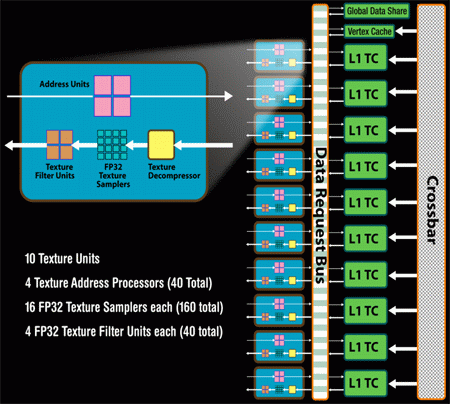
Their design has been completely redesigned, and now each TMU contains 16 FP32 texture fetch units, 4 address units, and 4 filter units. It would seem that the sampling efficiency should drop, however, this is compensated by the doubled bandwidth of the bus connecting the TMU and texture caches. ATI managed to achieve a 2.5x increase in the filtering speed for 32-bit textures and 1.5x for 64-bit textures, which looks very good in theory, and will most likely have a very positive effect on the performance of the new GPU in real conditions.
Texture processors are still combined into large modules of 4 TMUs, and each such module serves one of the 10 SIMD cores. Optimization, expressed in the rejection of unnecessary blocks, made it possible to reduce the number of transistors that make up the TMU, and, accordingly, place a larger number of them on a chip with relatively little bloodshed, while keeping the complexity and area of the core within reasonable limits.
The cache subsystem is an important part of the GPU texture subsystem, and in the RV770 it has also undergone a significant upgrade:
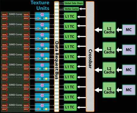
First of all, we should note the increased bandwidth: now the texture fetch rate from the first level caches is an impressive 480 GB/s, while the first and second levels caches can communicate at a speed of 384 GB/s. Secondly, each SIMD core now has its own first-level cache, which has a beneficial effect on data storage efficiency. Thirdly, second-level caches are coordinated with memory controllers, and, finally, fourthly, RV770 has a separate cache for storing vertex data. The improvements are not as obvious as in the case of the texture processor architecture, however, they will certainly make a significant contribution to the performance boost of the ATI Radeon HD 4800 in games. It's safe to say that the new ATI graphics processor is completely free from the main bottleneck of the ATI Radeon HD architecture and can now compete on equal terms with Nvidia solutions where the latter were traditionally strong, namely, in operations with textures. Here, ATI's approach to designing GPUs is most clearly manifested - optimization instead of direct increase in power.
Raster processors, referred to as render back-ends in ATI terminology, have never been a dramatic bottleneck in the ATI Radeon HD architecture, however, they have been improved in the RV770, although the total number of these modules has not changed: there are still four of them in the core, which allows us to talk about the equivalent of 16 classic ROPs.
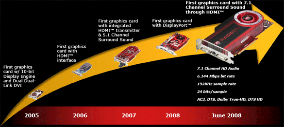
In addition to other innovations included in the ATI RV770, we should note new features of the video engine, in particular, a new sound controller and some software improvements.
Realtek's eight-channel audio controller, which supports audio streams up to 6.144 Mbps and 192 kHz sampling rates in AC3, DTS, Dolby True-HD and DTS-HD formats, is the main HD content enhancement. The enhanced capabilities of the new audio core are of great importance to those who plan to use the ATI Radeon HD 4000 as part of a home multimedia center. What's more, ATI's Radeon HD 4800s are currently the only graphics cards in the world to natively support 8-channel HD audio, with the ability to output it via HDMI - a significant advantage over competing Nvidia solutions.
To power the Radeon HD4870 video card, there are two 6-pin connectors in the tail of the video card, unlike the younger Radeon HD4850, which has only one connector. A reinforced power system was required for the stable operation of the video card at higher frequencies. So, compared to the Radeon HD4850 video card, the Radeon HD4870 GPU frequency is 125 MHz higher and equal to 750 MHz, and the effective GDDR5 video memory frequency is 3600 MHz, which is significantly higher than 1986 MHz, which is used by the video memory of the Radeon HD4850 video card. True, it’s worth making a reservation here, the real frequency of the new GDDR5 memory is 900 MHz, it’s just that in one clock cycle it transfers not twice, but four times more information compared to “ordinary” non-DDR memory.
Specifications ATI Radeon HD 4870
| Name | Radeon HD 4870 |
| Core | RV770XT |
| Process technology (µm) | 55 |
| Transistors (million) | 956 |
| Core frequency | 750 |
| Memory frequency (DDR) | 900 (3600 QDR) |
| Bus and memory type | GDDR5 256-bit |
| Bandwidth (Gb/s) | 115.2 |
| Unified shader blocks | 800 |
| Frequency of unified shader units | 750 |
| TMU per conveyor | 40 |
| ROP | 16 |
| Shader Model | 4.1 |
| Fill Rate (Mtex/s) | 30000 |
| DirectX | 10.1 |
| Memory | 512/1024 |
| Interface | PCIe 2.0 |
The Radeon HD4870 video card turned out to be not only in words, but in fact the most real competitor for the GeForce GTX 260 video card from NVIDIA. We have not seen this for a long time, because the "top" representatives of the two previous families of video cards from AMD could compete with NVIDIA products only in words, but in reality they were too slow. Obviously, the new shader unit with an increased number of stream processors and a changed architecture turned out to be more powerful than the shader unit in the GeForce GTX 260 video card. True, the new product falls short of the GeForce GTX 280, but at the same time it provides comfortable gameplay in almost all modern games.
mass effect