


Radeon R9 290X
The new Hawaii graphics chip at the heart of the AMD Radeon R9 290X graphics card is based on the Graphics Core Next (GCN) architecture that we already know, which has been slightly modified for computing capabilities and to fully support all DirectX 11.2 features, as previously done in chip Bonaire (Radeon HD 7790), which also became the basis for the Radeon R7 260X. The architectural changes in Bonaire and Hawaii relate to improvements in computing capabilities (support for more concurrently executing threads) and a new version of AMD PowerTune technology, which we will talk about more below.
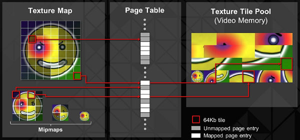
New features in DirectX 11.2 include tile resources that use Hawaii's GPU virtual memory hardware called partially-resident textures (PRT). Using virtual video memory, it is easy to obtain efficient hardware support for algorithms that allow applications to use huge amounts of textures and stream them into video memory. PRT allows for more efficient use of video memory in such tasks, and similar techniques are already being used in some game engines.
While the GCN capabilities have been expanded, AMD's main focus in designing the new top-end GPU was to improve the chip's power efficiency, as Tahiti was already consuming too much power, and Hawaii included more compute units. Let's see what AMD engineers managed to do to put a competitive product on the market:
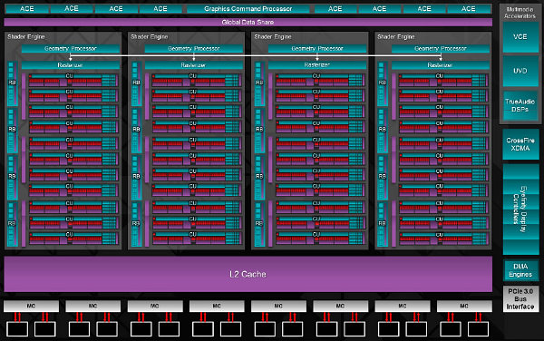
The new graphics processor is logically divided into four parts (Shader Engine), each of which contains 11 enlarged computing units (Compute Unit), including texture modules, one geometric processor and a rasterizer, as well as several ROP units. In other words, the block diagram of the most modern AMD chip has become even more similar to the diagram of NVIDIA chips, which also have a similar organization.
In total, the Hawaii graphics chip includes: 44 Compute Units containing 2816 stream processors, 64 ROPs and 176 TMUs. The GPU in question has a 512-bit memory bus consisting of eight 64-bit controllers, as well as 1 MB of L2 cache. It is produced on the same 28 nm process technology as Tahiti, but already contains 6.2 billion transistors (Tahiti has 4.3 billion).
Consider a block diagram of the shader engine that makes up the Hawaii GPU. This is a large-block part of the chip, which contains four of these engines:
Each Shader Engine includes one geometry processor and one rasterizer, which are capable of processing one geometry primitive per clock. It looks like Hawaii's geometric performance has not only improved, but should be well balanced compared to AMD's previous GPUs.
A GCN architecture shader engine can contain up to four enlarged Render Back-ends (RB) blocks, which include four ROP blocks each. The number of Compute Units in the shader engine can also be different, but in this case there are 11 of them, although the caches for instructions and constants are divided for every four Compute Units. That is, it would be more logical to include not 11, but 12 computing units in the Shader Engine, but it seems that such a number was no longer included in Hawaii's power consumption limits.
The computing unit of the GCN architecture includes various functional units: texture fetch modules (16 pieces), texture filtering modules (four pieces), a branch prediction unit, a scheduler, computational units (four vector and one scalar), first-level cache memory (16 KB per Compute Unit), memory for vector and scalar registers, and shared memory (64 KB per Compute Unit).
Since there are four shader engines in the Hawaii GPU, in total it has four geometry processing units and rasterization engines. Accordingly, AMD's new top-end GPU can process up to four geometric primitives per clock. In addition, geometry data buffering has been improved in Hawaii and caches for geometric primitive parameters have been increased. All together, this provides a significant increase in performance with large volumes of calculations in geometric shaders and the active use of tessellation.
Also, some changes have been made to the computing capabilities of the new, albeit graphical, but still processor. The chip includes two DMA engines that provide full use of the PCI Express 3.0 bus capabilities, a bidirectional bandwidth of 16 GB / s is declared. The possibility of asynchronous computing, which is carried out using eight (in the case of the Hawaii chip) Asynchronous Compute Engines (ACE), can also be called relatively new.
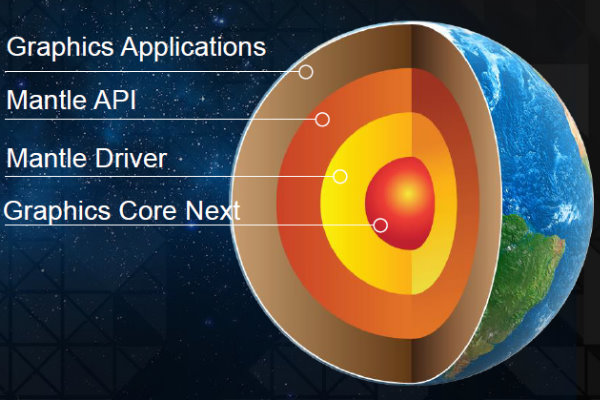
ACE blocks work in parallel with the GPU and each of them is capable of managing eight instruction streams. Such an organization provides independent scheduling and operation in a multitasking environment, access to data in global memory and L2 cache, as well as fast context switching. This is especially important in computing tasks, as well as in gaming applications when using the GPU for both graphics and general computing. Also, this innovation could theoretically be an advantage when using low-level access to GPU capabilities using APIs such as Mantle.
Let's get back to Hawaii's features that apply to graphical computing. Due to the increase in resolution requirements with the expected spread of UltraHD monitors, it becomes necessary to increase the computing power of raster operations units - ROP. The Hawaii chip includes 16 Render Back End (RBE) blocks, which is twice as many as Tahiti. Sixteen RBEs contain 64 ROPs, which are capable of processing up to 64 pixels per clock, and this can be very useful in some cases.
As for the memory subsystem, Hawaii has 1 megabyte of L2 cache, which is divided into 16 sections of 64 KB. Claimed as a 33% increase in cache memory, and an increase in internal throughput by a third. The total throughput of L2 / L1 caches is declared equal to 1 TB / s.
Memory is accessed via eight 64-bit controllers, which together make up a 512-bit bus. The memory chips in the Radeon R9 290X are clocked at 5.0 GHz, giving a total memory bandwidth of 320 GB/s, over 20% higher than the Radeon HD 7970 GHz. At the same time, the chip area occupied by the memory controller was reduced by 20% compared to the 384-bit controller in Tahiti.
Radeon R9 290X Specifications
| Name | Radeon R9 290X |
| Core | Hawaii |
| Process technology (µm) | 0.028 |
| Transistors (million) | 6200 |
| Core frequency | 1000 |
| Memory frequency (DDR) | 5000 |
| Bus and memory type | GDDR5 512-bit |
| Bandwidth (Gb/s) | 320 |
| Unified shader blocks | 2816 |
| Frequency of unified shader units | 1000 |
| TMU per conveyor | 176 |
| ROP | 64 |
| Fill Rate (Mpix/s) | 64600 |
| Fill Rate (Mtex/s) | 176400 |
| DirectX | 11.2 |
| Memory | 4096 |
| Interface | PCI-E 3.0 x16 |
Compared to its predecessor Radeon HD 7970, the performance of Hawaii in the face of the Radeon R9 290X will increase by about 40-60%.