


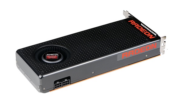
Radeon R9 380
At the heart of the Radeon R9 380 is the Antigua GPU, which is actually an update to the familiar Tonga chip (Radeon R9 285). It has not undergone any architectural changes. AMD has only optimized the power consumption of the GPU, most likely through a manufacturing process that allows for more chips that can run at lower voltages. The resulting power reserve was spent on increasing the operating frequency from 918 to 970 MHz.
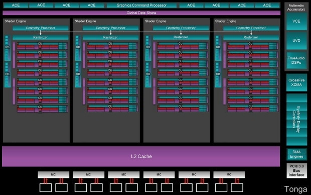
The Antigua chip, which is bundled with the Radeon R9 380, is similar in terms of the configuration of computing units (1792 shader ALUs, 112 texture units, 32 ROPs) to the "cut" Tahiti chip in the Radeon R9 280, and before it - the Radeon HD 7950, but differs in a narrower 256 -bit memory bus.
However, this version of Antigua/Tonga is also not fully functional. By itself, this is a larger ASIC compared to Tahiti (5 billion and 4.313 billion transistors, respectively), physically it contains the same number of computing units (2048 shader ALUs, 128 texture units) and has the same memory bus configuration (6 controllers, total bit depth - 384 bits). Thus, AMD left room for a potential Radeon R9 380X built on a fully unlocked version of the Antigua/Tonga GPU.
Radeon R9 380 Specifications
|
|
||||||
|
Chip
|
||||||
|
Frequencies
|
||||||
|
Memory
|
||||||
|
Interface and TDP
|
Another change in the specifications of the Radeon R9 380 compared to the R9 285 is that the memory bandwidth has been increased from 5500 to 5700 Gb / s, and the volume can reach 4 GB.