


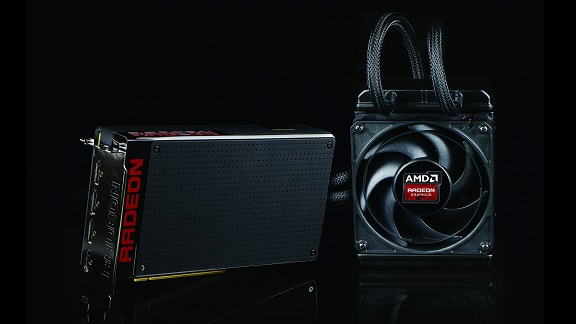
Radeon R9 Fury X
Fury X is the first solution to use the new type of High Bandwidth Memory. HBM memory outperforms GDDR5 memory in every way, offering more bandwidth with lower power consumption and a much smaller physical size, helping to accommodate smaller form factors.
The Fiji GPU, on which the new graphics card is based, uses TSMC's old proven 28nm process, as the transitional 20nm process did not live up to expectations, providing little improvement over 28nm.
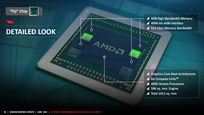
Fiji has become the largest ASIC released by AMD. The die area is 596 mm2, which is 36% larger than the area of Hawaii (438 mm2) and almost equals the area of NVIDIA GM200 (601 mm2).
AMD has never released internal naming of GCN interim versions, but Fiji falls into the category unofficially referred to as GCN 1.2 based on the combination of features. GCN, first introduced in the Tahiti GPU (Radeon HD 7970), has a dual purpose: 3D graphics rendering and, to no lesser extent, general purpose computing (GP-GPU). The last feature is due to the presence of hardware schedulers in the kernel, as well as the potential ability of all GCN-based ASICs to perform double precision (FP64) operations at a speed of 1/2 from FP32.
Both features eat up a significant portion of the processor's transistor budget, which makes it quite impressive that AMD has been able to scale chips up to 8.9 billion transistors without deviating from the principles laid down in the early days of GCN. FP64 performance in consumer products based on Fiji is limited to 1/16 of FP32, but AMD will certainly release FirePro accelerators that will fully exploit the capabilities of the new ASIC.
From GCN 1.1 products, Fiji inherited flexible GPU frequency and voltage control, an XDMA block that provides synchronization of multiple GPUs in CrossFre via the PCIe bus, and TrueAudio audio DSP.
Version 1.2 brought performance optimizations to GCN for geometric processors, as well as a new loseless color compression format, which saves memory bus bandwidth. In addition, it became possible to encode and decode H.264 video with Ultra HD resolution.
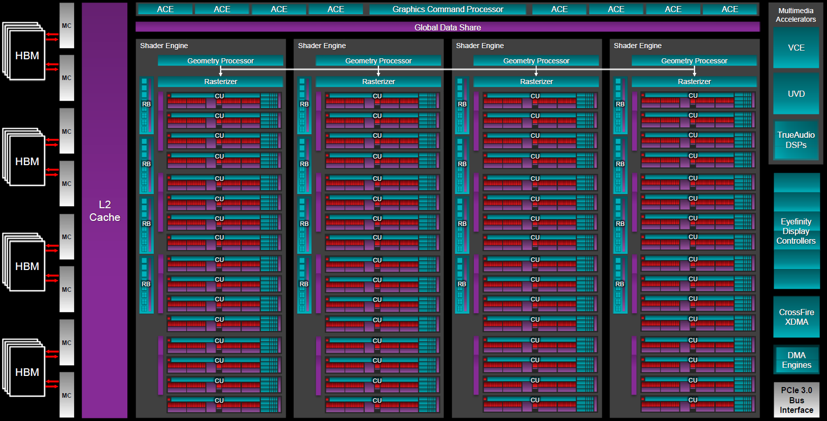
Based on the configuration of the computing units, Fiji is most easily described as a double Tahiti. Fiji and Hawaii are in a 16:11 ratio (~45% increase) in terms of the number of shader ALUs (stream processors) and texture units.
Such an unusual ratio in the configuration of shader ALUs and texture units in Hawaii and Fiji looks suspicious. And for good reason. From the Fiji block diagram, you can see that the number of the largest GPU building blocks, the Shader Engine, is still four, but the size of each has increased. Thus, the front-end of the chip, which performs triangle rasterization, becomes its bottleneck.
HBM is a joint project between AMD and SK Hynix, which should solve both problems through two technologies: a) packing RAM chips into a three-dimensional "stack"; b) connection with the GPU via a silicon substrate (interposer).
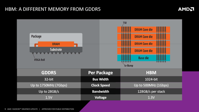
As for the multilayer packaging of microcircuits, conductors that allow connecting two silicon chips located one above the other are no longer something surprising. Hynix's innovation lies in the conductors passing through several layers of silicon - TSVs (Through-silicon vias).
The silicon interposer, oddly enough, is a less sophisticated technology. This "gasket" is made on standard photolithographic equipment, but this does not require advanced technologies - a standard of 65 nm is enough. Silicon itself here only plays the role of a substrate in which copper compounds are laid. Then, on microscopic metal balls (microbumps), formed in the places where the compounds come to the surface, multilayer chips HBM and ASIC Fiji are installed.
The HBM implementation for Fiji-based products includes four "stacks" of 1 GB each, connected to the GPU by a 4096-bit bus. The chips operate at 500 MHz with DDR technology (1 Gbps per lane). Thus, the resulting interface bandwidth reaches 512 Gbps.
Specifications Radeon Radeon R9 Fury X
|
|
||||||
|
Chip
|
||||||
|
Frequencies
|
||||||
|
Memory
|
||||||
|
Interface and TDP
|
The Fury X comes with a fully functional Fiji chip and an official TDP of 275W. The upper limit of the GPU clock frequency is 1050 MHz. Since the HBM memory chips are installed on a common substrate with the GPU, all that is on the PCB outside is the power system and I / O ports. Therefore, the Radeon R9 Fury X has surprisingly modest dimensions for a video card of this class, even more modest because AMD used a compact water cooling system instead of an air cooler.