


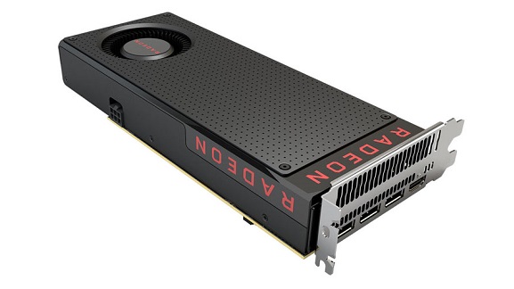
Radeon RX 480
At the heart of the Radeon RX 480 is the Polaris 10 GPU, which has the fourth generation GCN architecture, which is similar in many details to previous AMD solutions.
The Polaris 10 GPU belongs to the fourth generation of the Graphics Core Next architecture, the most advanced at the moment. The basic building block of the architecture is the Compute Unit (CU), from which all AMD GPUs are assembled.
The full Polaris 10 GPU includes one Graphics Command Processor, four Asynchronous Compute Engines (ACEs), two Hardware Schedulers (HWS), 36 Compute Units (CUs), four geometry processors, 144 texture a TMU (comprising four LSUs per TMU) and 32 ROPs.

With 5.7 billion transistors, the Polaris 10 die has an area of 232 mm2, which allows us to estimate an increase in chip density of 65% compared to Fiji, AMD's densest 28 nm GPU (8.9 billion transistors, 596 mm2) . For comparison, NVIDIA increased the density by 72% during the transition to the 16 nm process technology (GM200 - 8 billion transistors and 601 mm2, GP104 - 7.2 billion transistors, 314 mm2).
AMD achieved a 1.7x best-case performance-per-watt increase over previous iterations of GCN (AMD took the Radeon R9 290 for comparison) through brute force alone, the 14nm FinFET process, power gating, and clock gating. from power supply and frequency reset of idle computing units). Additional power management features have increased the declared result to 2.8.
AMD's new GPU memory subsystem includes eight 32-bit GDDR5 memory controllers, sharing a 256-bit memory bus, and 2MB L2 cache.
Radeon RX 480 Specifications
|
|
||||||
|
Chip
|
||||||
|
Frequencies
|
||||||
|
Memory
|
||||||
|
Interface and TDP
|
Reference RX 480 GPU clock speeds capped at 1266 MHz. The RX 480 uses GDDR5 chips with 8 Gb/s per pin for RAM, the highest speed available for this type of memory today.

The GCN architecture initially had the most complete set of features that the DirectX 12 API brought, and in the second generation (Hawaii and Bonaire chips, which are bundled with the Radeon HD 7790, R9 260/260X and R9 360) satisfies the conditions of feature level 12_0.
GCN version 1.3 of all features not covered in past iterations introduced support for calculating half precision (FP16).