


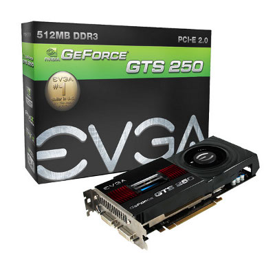
GeForce GTS 250
In December 2007, NVIDIA released the GeForce 8800 GTS 512 Mb video card based on the same G92 video chip. Unlike the similarly named GeForce 8800 GTS 640(320) MB based on the G80 GPU, they had:
more shader processors (128 vs 96), texture units (64 vs 48) and higher core clock (650MHz vs 513MHz), shader domain (1625MHz vs 1188MHz), GDDR (1940MHz vs 1584MHz).
GeForce 8800 GTS 512 Mb outperforms GeForce 8800 GTS 640 Mb without any problems due to the larger number of functional blocks and increased frequencies. Moreover, he was able to overtake the undefeated GeForce 8800 GTX 768 Mb until that moment. Thanks to this and the lower price, this video card became a real hit among gamers of the time.
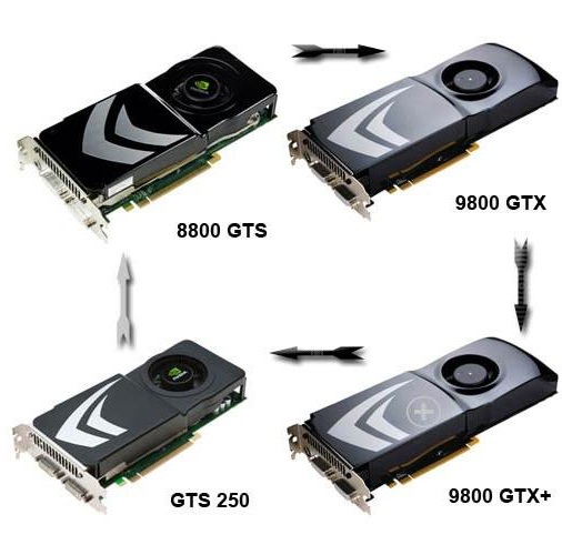
In April 2008, NVIDIA released the video card GeForce 9800 GTX 512 Mb. It differed from the GeForce 8800 GTS 512 Mb in a longer printed circuit board, an increase in the number of power connectors from one six-pin to two, and increased core/shader domain/video memory frequencies. Thanks to the increase in frequencies, the GeForce 9800 GTX 512 Mb managed to catch up with the previous flagship GeForce 8800 Ultra 768 Mb in terms of performance.
At the same time, the entire 88xx line of video cards was rebranded:
the GeForce 9800GT replaced the GeForce 8800 GT;
GeForce 9800GTX replaced GeForce GeForce 8800 Ultra 768 Mb;
The GeForce 8800GTS 512 MB was discontinued in order not to compete internally with the stronger GeForce 9800 GTX 512 MB.
In May 2008, the GeForce GTX 260 and GeForce GTX 280 video cards were announced. These video cards occupied the Hi-end sector of the market. The 98xx line has moved to the middle-end sector.
At that moment, NVIDIA dominated all sectors of the video card market, and nothing seemed to threaten its position. AMD was then in an unenviable position: processors were losing to Intel products on all fronts, the situation with video cards was no better. On the way there were HD4xxx video cards based on the RV770 video chip. But no one believed in them, the reputation of the Radeon brand suffered too much due to the failed HD2xxx and unsuccessful HD3xxx lines.
But then a bolt from the blue struck - the RV770 video chip, underestimated by NVIDIA, turned out to be very successful. The younger Radeon HD 4850 was able to compete on equal terms with the GeForce 9800 GTX, and the older Radeon HD 4870 outperformed the GeForce GTX 260 in many cases. At the same time, the prices for these video cards were almost two times lower than their competitors. Plus, AMD engineers completely redesigned the RV770 architecture and presented the world with a very strong video chip. The most striking impression from these video cards was the forcing of full-screen anti-aliasing in games:
when forcing AA4, the performance of the video card fell by only 20-25%;
forcing AA8 was generally considered practically free.
And these impressions were more vivid, considering that everyone still had fresh memories of a twofold drop in the performance of HD2xxx/HD3xxx video cards even when AA2 was forced.
The situation for NVIDIA is extremely difficult. She urgently had to reduce prices for her products to competitive ones (many users should remember about the double price drop for the GeForce 9800 GTX right after the announcement of the Radeon HD 4850).
Nevertheless, NVIDIA managed to get out of this situation with honor. Already in the summer of 2008, it launched the 55nm G92b video chip and the George 9800 GTX+ video card based on it with increased core/shader domain/video memory frequencies. This accelerator managed to catch up and overtake the Radeon HD 4850.
And in the spring of 2009, NVIDIA again started a rebranding, deciding to rename the GeForce 9800 GTX + to GeForce GTS 250. Thus, NVIDIA fits the entire current video card model range under one trade line.
Specifications NVIDIA GeForce GTS 250
| Name | GeForce GTS 250 |
| Core | G92b |
| Process technology (µm) | 0.055 |
| Transistors (million) | 754 |
| Core frequency | 738 |
| Memory frequency (DDR) | 1100 (2200) |
| Bus and memory type | GDDR3 256-bit |
| Bandwidth (Gb/s) | 70.4 |
| Unified shader blocks | 128 |
| Frequency of unified shader units | 1836 |
| TMU per conveyor | 64 |
| ROP | 16 |
| Shader Model | 4.0 |
| Fill Rate (Mpix/s) | 11808 |
| Fill Rate (Mtex/s) | 47232 |
| DirectX | 10.0 |
| Memory | 512.1024.2048 |
| Interface | PCIe 2.0 |