


GeForce GT 430
The internals of the GF108 chip are two clusters of shader units of the GF104/106 version, with 48 shader processors and 8 TMUs each. Although, contrary to fears, NVIDIA did not cut geometry performance, retaining one Polymorph Engine block per cluster, ROP blocks were “castrated” - instead of the principle “8 ROPs per 64-bit bus”, only 4 ROP blocks were left in GF108. This means that the already modest theoretical performance of the solution in real applications will be absolutely terrible.
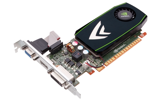
The reference design has a 1U-oriented design, DVI, HDMI and VGA ports, an active cooling system, but end card manufacturers will certainly offer their own solutions, including those with passive cooling. The power consumption of the card is very modest, the card does without a power boost, and SLI support is considered excessive functionality for an entry-level.
Specifications NVIDIA GeForce GT 430
NameGeForce GT 430CoreGF108Technical process (µm)0.04Transistors (million)?Core clock700Memory clock (DDR)900 (1800)Bus and memory typeGDDR3 128-bit bandwidth (Gb/s)28.8Unified shader units96Unified shader unit frequency1400TMU per pipeline16RO P16Shaders Model5.0Fill Rate( Mpix/s)11200Fill Rate (Mtex/s)11200DirectX11.0Memory1024Interface PCI-E 2.0 x16
In general, the new solution is an analogue of the GeForce GT 240 with a new architecture and support for DirectX 11/OpenGL 4/CUDA compute capability 2.1, but a closer look will immediately reveal that the novelty differs in a number of parameters, including video memory bandwidth and scene fill rate. not for the better. With this strategy, it will be extremely difficult to beat competing AMD Radeon solutions in the same price range (recommended price - $ 79).