


GeForce GTX 960
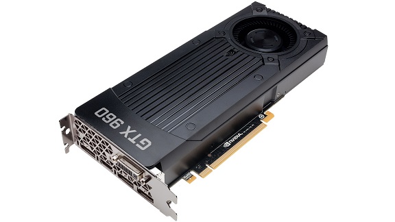
With the GeForce GTX 960 graphics card, NVIDIA brought the benefits of the "Maxwell" architecture to the mainstream market. Video cards have received such architectural advantages as memory compression, DSR, MFAA, VXGI and DirectX 12. For NVIDIA, its own GameWorks and PhysX APIs are becoming increasingly important, there is no news about this yet, but buyers of the GeForce GTX 960 will also benefit from their support.
The GeForce GTX 960 video card uses the GM206 GPU, probably not in its full version - under the GM206-300-A1 marking. The chip is equipped with 2.94 billion transistors, it is significantly less complex than "Tahiti" or "Tonga" from AMD. Since the reference GeForce GTX 960 graphics card is not presented, the information about the base frequency and Boost in the table above is of no practical importance. NVIDIA lists a base clock of 1.126 MHz and a GPU Boost clock of 1.178 MHz. NVIDIA set 2.048 MB of GDDR5 memory to 1.750 MHz, the memory is connected via a 128-bit interface. The result is a memory bandwidth of 112.2 GB/s, which is not much compared to the competition. But don't forget that NVIDIA uses a memory compression technology that theoretically increases the effective memory bandwidth, but the promised NVIDIA 148,
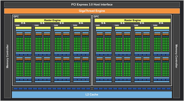
The GM206 GPU is based on 1.024 stream processors, which are combined into eight SMM blocks (streaming multiprocessors), 4x 32 stream processors each. Four SMMs make up a GPC cluster, we get two such clusters per GPU. 8 (SMM) x 4 (SMM units) x 32 stream processors just gives 1,024 stream processors.
Each SMM uses eight texture units. Accordingly, eight SMMs in the GeForce GTX 960 give 64 texture units. Two 64-bit memory controllers are connected to 32 raster operations pipelines (ROPs).
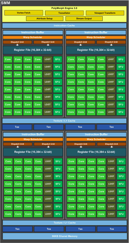
NVIDIA was able to achieve higher efficiency of Maxwell thanks to several solutions. The L2 cache in the "Maxwell" architecture has been increased to 2.048 KB compared to 256 KB in the "Kepler" architecture. The cache bandwidth remained at 512 bytes per clock. Compared to the first generation Maxwell architecture, the total memory for each SMM has been slightly increased. Now it is already 96 kb, not 64 kb. We can also note the new Polymorph Engine version 3.0.
The PolyMorph 3.0 engine is responsible for texture queries, tessellation, attribute setting, field of view transformation, and streaming output. The results of the calculations of the SMM cluster and the PolyMorph 3.0 engine are then passed to the rasterization engine. At the second stage, the tessellator starts calculating the positions of the surfaces, depending on the distance, the required level of detail is selected. The adjusted values are sent to the SMM cluster, where domain and geometry shaders work with them. The domain shader calculates the final position of each triangle based on Hull shaders and tessellators. At this stage, displacement maps are superimposed. The geometry shader then compares the calculated data with the actually visible objects and sends the results back to the tessellation engine for final calculation. At the last stage, the PolyMorph 3. 0 performs field of view transformation and perspective correction. Finally, the calculated data is output via stream output, the memory is freed for further calculations.
Let's move on to the individual blocks of the SMM multiprocessor. Each block of 32 stream processors is equipped with an instruction buffer and a warp scheduler. The two dispatchers work with 16.384 32-bit registers each. Looking at the "Kepler" architecture, there were 192 stream processors running four warp schedulers and eight dispatch units, for a total of 65,536 32-bit registers. Theoretically, for each stream processor in the Maxwell architecture, there are 512 registers, in Kepler their number was about 341. This measure also contributed to an increase in the performance of stream processors up to 35%.
Specifications GeForce GTX 960
|
|
||||||
|
Chip
|
||||||
|
Frequencies
|
||||||
|
Memory
|
||||||
|
Interface and TDP
|
Also, the ratio between stream processors and the so-called special functional units (Special Function Units, SFU) has changed somewhat. In the "Kepler" architecture the ratio was 6/1, in "Maxwell" it dropped to 4/1. The same applies to the ratio of stream processors and read/write units (Load/Store, LD/ST). Special double-precision calculation blocks are not shown in the diagram, they will most likely be presented in the GM210 GPU (similar to GK110 and GK104). But, according to NVIDIA, the ratio of single and double precision is 1/24, just like in the first generation "Kepler" chips (GK104).
Small changes compared to the previous implementation of the "Maxwell" architecture have taken place in the video processing engine (Video Engine). Now it provides not only hardware encoding in H.265, but also hardware decoding. The GeForce GTX 980 and GeForce GTX 970 also lacked HDCP support in HDMI 2.2, while the GeForce GTX 960 and the GM206 GPU added it.