


Radeon HD 6970
It's been a little over a month since Advanced Micro Devices introduced Barts-based Radeon HD 6800 mid-range graphics cards, and the company is now releasing two of its most powerful Cayman-powered single-socket solutions.
Although the new Cayman GPUs belong to the HD 6xxx series, they differ architecturally from the HD 68xx solutions and, of course, from the HD 58xx. These differences are both quantitative and qualitative in nature, and are an important step in the development of the new AMD graphics architecture.
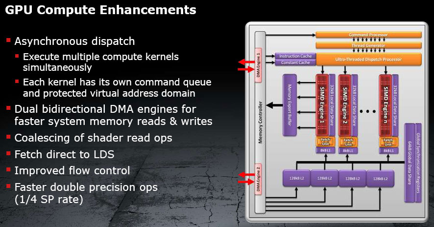
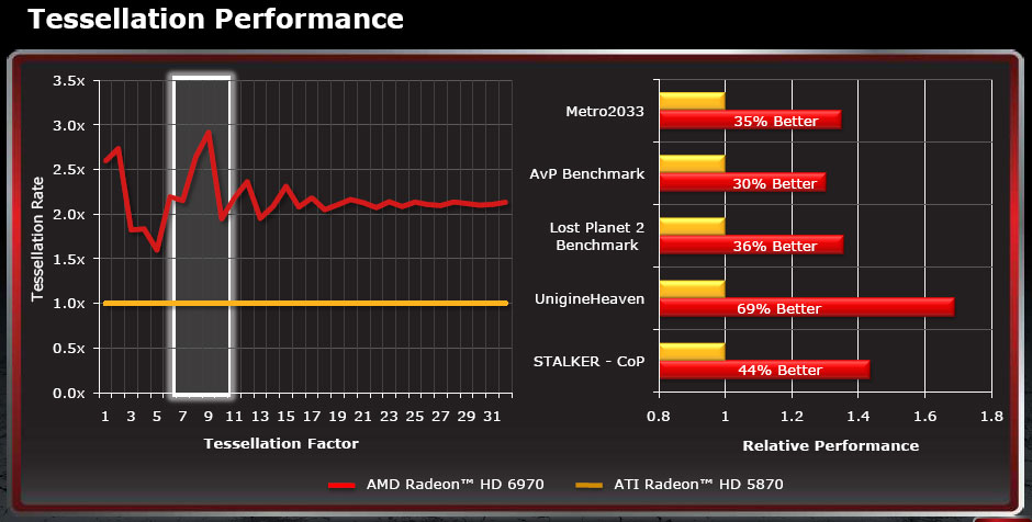
The new GPUs have increased the speed of working with double precision operations and optimized the mechanism for exchanging with system memory. Of the other equally important Cayman improvements, we can name an increase in the performance of raster operations units (ROP) in a number of modes, and the traditional improvement of the tessellation unit, which , according to AMD, has become significantly faster than its predecessor:
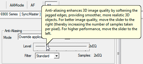
The rest of the Cayman GPU changes are quantitative. Thus, the number of texture sampling and filtering units was increased from 80 to 96, the number of VLIW processors increased, compared to Cypress, from (1600/5) 320 pieces to (1536/4) 384 pieces, i.e. by 20%. In addition to the morphological anti-aliasing previously introduced in the Radeon HD 68xx series, the Radeon HD 69xx has a new anti-aliasing algorithm - the so-called "Enhanced Quality AA", which is an addition to MSAA and is activated in the Catalyst driver control panel (EQ):
Through this setting, you can change the peak power limit of the video card, and thereby either save electricity, or, in other words, increase the likelihood of successful overclocking of the GPU. The new Cayman GPUs now have multiple sensors that continuously monitor the GPU's health and utilization, allowing Caymans to operate more efficiently. In addition, these sensors in the GPU, when programs like FurMark and the like are detected, will activate the protection mode, putting the card into a kind of throttling mode, periodically reducing the chip frequency.
And vice versa - you can lower the maximum energy power of the video card by setting negative values of this setting. In this case, there will be a drop in performance. However, again, according to AMD, it will not be critical:
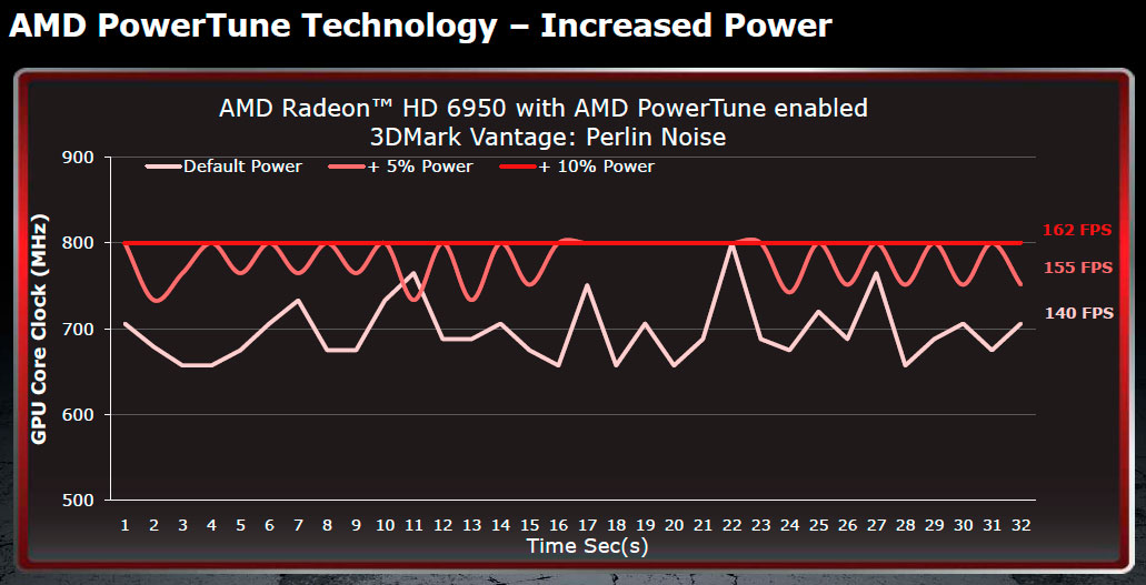
The power control limits are programmed in the BIOS of the video card, and we hope that over time there will be tools for expanding them (primarily upwards, of course). In this case, when organizing effective cooling of the GPU, it will be possible to avoid the limitations of the overclocking potential of the video card by the upper limit of throttling.
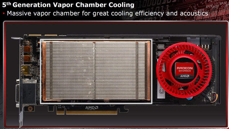
To remove heat from the Radeon HD 6950/6970, the manufacturer used a cooling system with an evaporation chamber. This is not the first time that AMD has resorted to using a similar design, and NVIDIA recently adopted this approach.
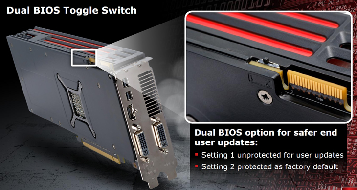
As you know, some video card manufacturers use two BIOS chips for their best solutions. This feature allows enthusiasts to more flexibly tune their accelerators without unnecessary risk of “killing” the card during flashing. From now on, this technology is implemented on serial AMD video cards. Reference versions of the AMD Radeon HD 6950/6970 are equipped with two BIOS chips, one of which is write-protected, while the other allows flashing. In our opinion, this is a very useful solution, especially for those who like to experiment with memory frequencies and timings.
AMD Radeon HD 6950/6970 accelerators look practically the same from each other, even the size of the boards is identical. Accelerators can be distinguished only by the sticker on the casing of the CO, as well as by the power connectors. The Radeon HD 6950 accelerator is powered by two 6-pin PCI-Ex connectors, while the Radeon HD 6970 requires one 6-pin and one 8-pin connector. On the reverse side of the board is almost completely covered with metal plates. Apparently, this was done to evenly distribute heat over the surface of the accelerator.

The flagship Radeon HD 6970 is positioned by the creators as the most attractive single-GPU model for computer enthusiasts and avid gamers, with a theoretical performance of up to 2.7 trillion floating point operations per second.

deocards are built on a chip manufactured using 40-nm technology with a die area of 389 mm2 (2.64 billion transistors), which, as we have already said, is known under the code name Cayman, and the older one is based on the Cayman XT version with 1536 stream processors, 96 texture modules (TMU) and 32 rasterization units (ROP).
| Radeon HD 6970 Specifications |
|
The Radeon HD 6970 is on par with the GeForce GTX 570 and GeForce GTX 480 in terms of performance, although many saw it as a competitor to the GeForce GTX 580 before the release. The only attractive feature compared to the competitor is its price, which is only $350, which is $150 lower than on GeForce GTX 580.